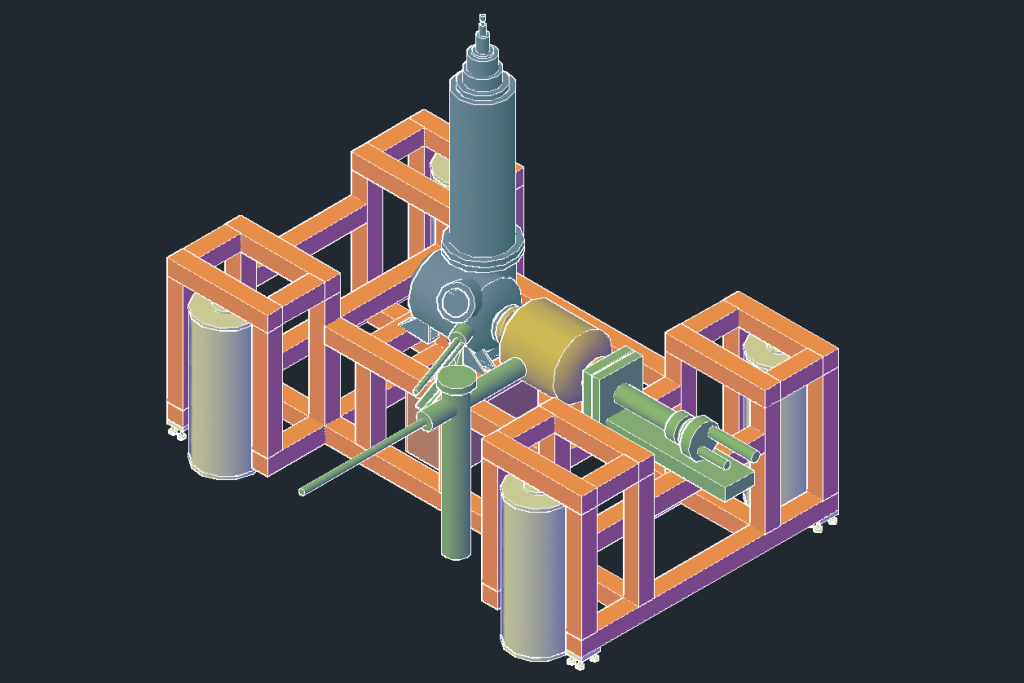
Our lab has state-of-the-art equipment for both device fabrication and atomic-scale imaging.
- 4 K 2 T UHV SPM system with multiple leads on both sample and probe sides
- UHV MBE chamber for thin film growth of S, Se, and Te-based compounds and metal alloys
- Ambient stacking stage for fabricating layered 2D materials and devices
