Our lab has state-of-the-art equipment for both device fabrication and atomic-scale imaging.
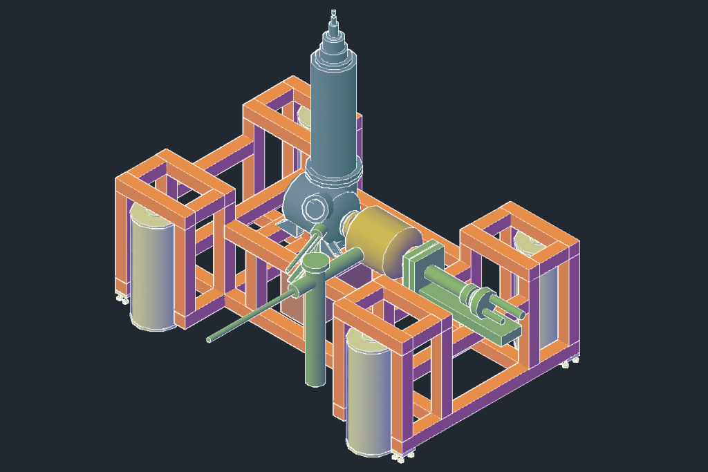
- 4 K 2 T UHV SPM system with multiple leads on both sample and probe sides
- UHV MBE set up for thin film growth of S, Se, and Te-based compounds and metal alloys
- Ambient stacking stage for fabricating layered 2D materials and devices
- Sputtering system for semiconductor deposition (shared)
- Thermal deposition chamber for metals (shared)
- Ambient Asylum MFP-3D AFM instrument (shared)
- Laser lithography tool (shared)
- Two reactive ion etching systems (shared)
Maxquantum also actively uses advanced characterization and nanofabrication tools in the CSU’s ARC facility.
